Product Overview
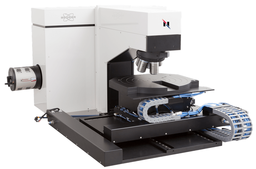
The Bruker RAMANdrive represents a significant leap in industrial spectroscopy, merging high-throughput performance with the precision of a research-grade Raman microscope. Engineered specifically for the semiconductor and materials science sectors, this system features a massive motorized sample stage with a 300 x 300 x35 mm dynamic range, accommodating full 12-inch wafers for comprehensive mapping and inspection. High-level efficiency is built into the hardware through a dedicated wafer navigation system and fully automated laser switching, which allows the system to transition between up to four excitation sources without manual intervention
The system’s versatility is anchored by its dual-illumination capabilities, offering both high-resolution point measurement and rapid line illumination modes. With a 550 mm focal length spectrograph and high-quantum-efficiency CCD detector, the RAMANdrive delivers exceptional spectral resolution and sensitivity across a wide range of excitation wavelengths. Whether performing 3D depth profiling or identifying unknown contaminants through customized spectral libraries, the RAMANdrive provides the robust data required for advanced process control and material characterization.
Beyond standard identification, the RAMANdrive excels in topographical Raman imaging, which automatically adjusts for uneven surfaces to ensure consistent focus across a large sample area. This capability is essential for analyzing modern semiconductor architectures where surface morphology can vary significantly. The software facilitates this through live multivariate imaging, calculating peak height, width, and position in real-time to generate instant chemical maps that allow operators to visualize material properties as they are being measured.
To maintain rigorous laboratory standards, the RAMANdrive is housed in a Class 1 laser safety enclosure and is compatible with cleanroom environments via an optional air filtering unit. The integration of an internal Neon lamp and Silicon reference allows for fully automated calibration, eliminating the drift and systematic errors often associated with long-term industrial use. By combining automated particle recognition with high-speed data acquisition, capable of 1330 spectra per second, the system transforms complex spectroscopic data into actionable insights for high-volume manufacturing.
Key Features
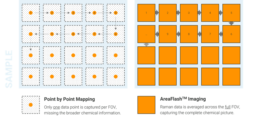
- Ultrafast Imaging: Acquires 400 spectra simultaneously for lightning-fast mapping.
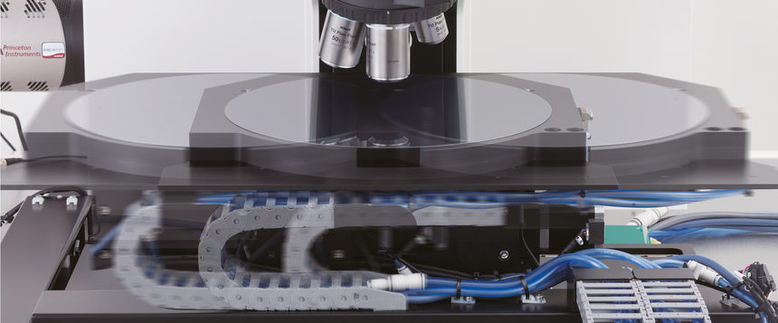
- 300 mm Wafer Stage: Fully automated, vacuum-secured navigation for large-scale substrates.
- AreaFlash™ Technology: Guarantees complete laser coverage for representative sampling without dead zones.
- Sub-100 nm Detection: High-sensitivity dark-field microscopy for locating nano-scale particles.
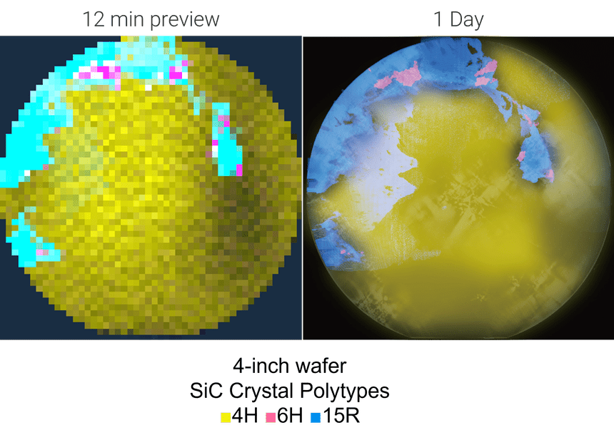
- Polytype Discrimination: Precise differentiation of SiC crystal structures (e.g., 4H vs. 6H).
- Automated Calibration: Internal quartz reference ensures continuous wavenumber accuracy.
Specifications
| Sample Compatibility | Up to 300 mm wafers (vacuum hold) |
| Spatial Resolution | Sub-micron (diffraction limited) |
| Excitation Lasers | Multi-wavelength options (inc. UV 325 nm for PL) |
| Imaging Speed | 400 spectra per laser shot |
| Calibration | Automated internal quartz reference (464 cm⁻¹) |
| Analysis Modes | Raman Imaging, Photoluminescence (PL), Dark-field |